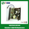
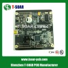
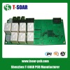
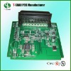
- Other PCB & PCBA[1]
- Multilayer PCB[10]
- Single-Sided PCB[2]
- Rigid PCB[2]
- Double-Sided PCB[4]
- FPC[7]
- Contact Person : Mr. Liu Simon
- Company Name : Shenzhen T-Soar Technology Co., Ltd.
- Tel : 0086-755-29473363
- Fax : 0086-755-29473512
- Address : Guangdong,Shenzhen,Dongbian commercial building,Minzhi Street, Longhua Town, Shenzhen China
- Country/Region : China
- Zip : 518109
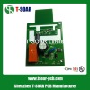
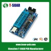
OEM/ODM PCB And PCB Circuit Assembly
PCB Circuit Assembly, PCB DIP, PCB SMT.
Welcome to T-SOAR PCB Manufacturer
---------------------------------------------------------------------------------------------
1> PCB Processing Details:
Place of Origin Shenzhen China (Mainland) | Brand Name: T-soar pcb | Model Number: 1 layers pcb |
Base Material: FR-4 | Copper Thickness:0.5 oz | Board Thickness: 1.2mm |
Min. Hole Size: 0.3mm | Min. Line Width: 4.5mil | Min. Line Spacing: 4.5mil |
Surface Finishing: HASL (Lead Free) | Soldermask: None | Legend: White |
Test: 100% E-testing | Purchase Components | Original Standard |
2> Package & Delivery:
Packing details: | Heat sealed packing, Vacuum packing, Export carton |
Delivery time: | 7-9 Days |
3> Detailed specification of manufaturing capacity:
NO | Item | Craft Capacity |
1 | Layer | 1-30 Layers |
2 | Base Material for PCB | FR4, CEM-1, TACONIC, Aluminium, High Tg MaterialHigh FrequenceROGERS ,TEFLON, ARLON, Halogen-free Material |
3 | Rang of finish baords Thickness | 0.21-7.0mm |
4 | Max size of finish board | 900MM*900MM |
5 | Minimum Linewidth | 3mil (0.075mm) |
6 | Minimum Line space | 3mil (0.075mm) |
7 | Min space between pad to pad | 3mil (0.075mm) |
8 | Minimum hole diameter | 0.10 mm |
9 | Min bonding pad diameter | 10mil |
10 | Max proportion of drilling hole and board thickness | 1:12.5 |
11 | Minimum linewidth of Idents | 4mil |
12 | Min Height of Idents | 25mil |
13 | Finishing Treatment | HASL (Tin-Lead Free), ENIG(Immersion Gold), Immersion Silver , Gold Plating (Flash Gold), OSP, etc. |
14 | Soldermask | Green, White, Red, Yellow, Black, Blue, transparent photosensitive soldermask, Strippable soldermask. |
15 | Minimun thickness of soldermask | 10um |
16 | Color of silk-screen | White, Black, Yellow ect. |
17 | E-Testing | 100% E-Testing (High Voltage Testing); Flying Probe Testing |
18 | Other test | ImpedanceTesting,Resistance Testing, Microsection etc., |
19 | Date file format | GERBER FILE and DRILLING FILE, PROTEL SERIES, PADS2000 SERIES, Powerpcb SERIES, ODB++ |
20 | Special technological requirement | Blind & Buried Vias and High Thickness copper |
21 | Thickness of Copper | 0.5-14oz (18-490um) |
4> Workshop Silhouette
5> Welcome to our Website: www. tsoar-pcb.com
OEM/ODM PCB And PCB Circuit Assembly

